Everlast Win Electronics CO., Ltd.
Products
Product Features
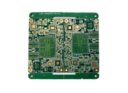
Multi-layer boards manufactured by Build Up process and blind/ buried via Micro-via, to achieve the characteristics of high-density wiring.
Micro-hole design (aperture <0.15mm), high wiring density
The minimum line width/ spacing for mass production is 0.076/ 0.076mm, and the sample line can reach 0.076/ 0.076mm.
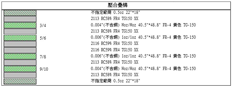
Variety of stacking structure, 1~26 layers can be processed (including Any-Layer), processing board thickness 0.25~4.0mm.
Diversified selection of raw materials, mainly halogen-free environmentally friendly materials.
HDI Application:
HDI PCB high-density connection board, currently can produce multi-level ANY LAYERS. Application areas: NB, Tablet Computers, Digital Cameras, Automotive Electronics.
-
Industrial Computer Products -
Currently, there is no product exhibited.
Please select another subcategory to view product details.
 All Categories